To outsiders, creating a charger or power adapter seems like a piece of cake: use a reference design, lay out the PCB, put it in a casing, and start selling. But anyone who has actually taken a product from zero to one knows that this journey is filled with endless trials and tribulations.
Today, we’re going to break down the major pain points and “fatal” pitfalls that hardware engineers and project managers frequently encounter during Fast Charger R&D. If you are currently stuck in these traps, don’t panic—you are not fighting alone.
🔌 Pain Point 1: The Endless “Seesaw” Between Safety Regulations and EMC
In power supply design, fixing one issue often creates another—much like a game of whack-a-mole. This is perfectly illustrated during EMI (Electromagnetic Interference) and safety debugging.
-
The Deadlock Between Leakage Current and EMI: During safety testing, we often find leakage current exceeding limits. The standard fix is adjusting the Y capacitor. However, once the leakage current drops, we test for EMC again, only to find that EMI radiation fails. Hardware engineers frequently have to bounce between Y capacitor voltage parameters, transformer shielding, and parasitic capacitance to find that extremely narrow sweet spot.
-
Conducted Emission Margins That Trigger OCD: Merely passing the test isn’t enough. Generally, if the conducted emission margin is less than 5dB, we feel very insecure. To ensure mass production consistency and avoid nasty surprises, we usually have to arrange for re-testing at a third-party laboratory.
💻 Pain Point 2: “Protocol Compatibility” Torments More Than Hardware
Today’s power adapters no longer just output raw voltage and current; they act more like miniature computers constantly “negotiating” with devices. The market is flooded with various protocols for phones, laptops, and tablets, making compatibility a huge hurdle in Fast Charger R&D.
-
The Infuriating “Intermittent Charging”: During prototype testing, we often encounter specific devices that suddenly stop charging halfway or repeatedly reboot the handshake process. This usually involves extremely low-level protocol communication details, requiring us to capture data packets, analyze waveforms, and modify code over and over until the issue is entirely resolved.
-
The “Trainwreck” of Power Downgrade Timing: When plugging or unplugging devices from a multi-port charger, dynamic power redistribution must occur. Many projects expose issues during testing where the timing of power downgrades is incorrect or the NTC (thermistor) thermal throttling logic isn’t smooth. If the timing is misaligned, either the device won’t charge, or the charger will trigger an over-temperature protection shutdown.
⚙️ Pain Point 3: “Edge Bugs” in Hardware-Software Synergy
Modern power supplies are becoming smarter. Beyond the core power delivery stage, a critical aspect of Fast Charger R&D is ensuring peripheral circuits and software coordination don’t drop the ball.
-
The “Temper Tantrums” of UI and Digital Displays: For chargers with displays or status LEDs, we frequently discover at the last minute that the HEX codes are wrong or the UI display logic has a bug. While this doesn’t affect charging, it severely impacts the user experience and often requires urgent calls to the software team for an overnight firmware update.
-
Repeated Prototyping of the Protocol Board: The mainboard might be perfectly fine, but the protocol daughterboard often requires repeated revisions due to issues like pin definitions or mismatched startup resistors. The daily routine becomes: spot a problem ➡️ urgently revise schematics ➡️ push for expedited prototyping ➡️ keep testing.
🚀 Pain Point 4: The Leap from the “Lab” to the “Assembly Line”
You might think it’s over once you’ve tuned all parameters in the lab. Unfortunately, the real test of mass production has just begun.
-
The Nerve-Wracking Validation of New Components: Every time a new component is introduced (like switching to a new 80mR GaN power IC), it must go through rigorous EVT (Engineering Verification Test). No matter how flawless the datasheet looks, you can’t draw a conclusion until you’ve run exhaustive stress tests on the actual physical board.
-
The Endless ECNs: From the lab to mass trial production, there are always countless details to perfect. Updating PCB files, adjusting the BOM (Bill of Materials), navigating the ECN (Engineering Change Notice) process… every single step is a race against time.
🌟 The Fruit of Our Labor: Built on Rigorous Testing
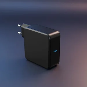
Because we understand these pitfalls so deeply, we leave no stone unturned when developing our own products. If you want to experience a product born from uncompromising standards and relentless debugging, check out our 67W GaN Fast Charger.
It has successfully passed stringent EMI limits, features seamless dynamic power distribution, and offers flawless compatibility across all major protocols.
R&D Reflections A so-called “Senior Hardware Engineer” is really just someone who has learned to find the balance between leakage current and EMI, decode the patterns in endless charging disconnection logs, and accumulate experience from countless prototypes. Behind every stable product lies a graveyard of burnt PCBs and the lost hair of engineers.
There are no shortcuts in Fast Charger R&D. To all the R&D brothers and sisters out there: respect the technology, and keep pushing forward through the pitfalls!