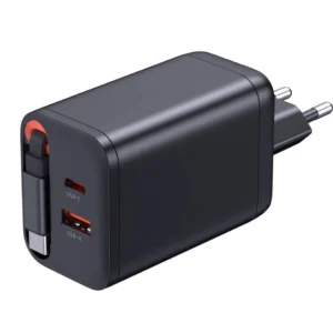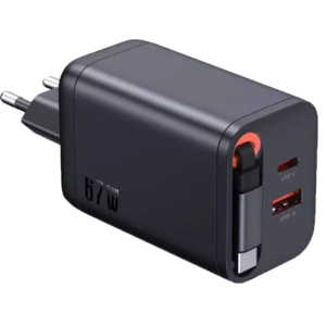
When sourcing premium power products globally, finding a reliable custom GaN charger OEM is critical. The biggest hidden risk for B2B buyers is rarely a cosmetic defect. It is usually “charging failure” due to protocol incompatibility, or worse, device damage caused by thermal control failure. For high-power devices, packing tens or even over a hundred watts of power into an incredibly compact size is not just a hardware engineering marvel—it is a massive test of underlying logic control for any custom GaN charger OEM.
Achieving true “100% safety and broad compatibility” requires much more than just premium components. The real core competency lies in the critical step immediately following PCBA assembly: Firmware Flashing (Programming).
Firmware: The True “Brain” of Fast Charging Devices
If the main control chip and transformer are the skeleton and muscles of a charger, the firmware code is its soul. Before moving to final testing, every device rolling off a custom GaN charger OEM production line must be injected with rigorously verified programming via professional offline flashing equipment. This code dictates exactly how the charger communicates with external devices at the base level.
Smart Power Allocation and Ultimate Compatibility
Modern users typically have a mix of devices from different brands on their desks, each utilizing distinct fast-charging protocols (e.g., PD 3.0/3.1, PPS, QC).
-
Precise Protocol Handshake: Through meticulous coding and flashing, engineers ensure that the moment the charger connects to a device, it instantly recognizes the target’s voltage and current requests, completing an accurate communication handshake in milliseconds.
-
Dynamic Power Distribution: As an experienced custom GaN charger OEM, we know that for multi-port devices, the firmware controls intelligent power allocation. When multiple devices are connected simultaneously, the underlying programming instantly recalculates and distributes the total wattage. This guarantees that all ports deliver optimal, safe efficiency, drastically reducing compatibility complaints from end-users.
Millisecond-Level Fail-Safe Protections
Under peak load conditions, safety is absolutely non-negotiable. Choosing a top-tier custom GaN charger OEM means not only getting high-spec hardware but also strict safety thresholds hardcoded directly into the programming.
-
Real-Time Thermal Monitoring: The firmware continuously reads data from the NTC thermistors on the PCBA. The moment internal temperatures approach safety limits, the program instructs the main control chip to throttle the output wattage or cut power entirely, eliminating overheating risks at the source.
-
Multiple Anomaly Blocks: Whether it is a sudden surge from the power grid or an unexpected short circuit on the output end, the protective logic embedded in the chip reacts in fractions of a second. This safety net, deeply rooted in the base code, serves as a solid defense for your brand’s reputation.
Rigorous Production Line Flashing and QC Standards
To perfectly execute R&D designs, a professional custom GaN charger OEM facility enforces a 100% firmware integrity verification process. Using professional programming tools, the code is accurately and consistently batch-written into every MCU chip.
Any PCBA that fails the code verification is automatically intercepted by the production line systems and will never proceed to final assembly. This model significantly elevates the yield rate and batch consistency for custom GaN charger OEM orders.
Partnering with a dedicated custom GaN charger OEM equipped with profound R&D capabilities means your brand receives comprehensive protection—from base code to final hardware assembly. This rigorous integration of software and hardware is the only path to delivering truly premium power products.